 Erencan Yılmaz
The global surge in AI chip demand has pushed Samsung to resume construction on its substantial Pyeongtaek Plant 5 (P5) facility, which had been on hold during the recent downturn in the semiconductor sector. With AI hardware requirements intensifying, Samsung is expediting preparatory work at its Pyeongtaek site, already recognized as the largest semiconductor production hub worldwide.
Samsung is working to make its Pyeongtaek Plant 5 facility operational
Originally, P5 was scheduled to break ground in 2024, but as market conditions shifted, Samsung temporarily scaled back capital investments. With the AI hardware market now accelerating, the company is fast-tracking development on P5 to enhance production capacity.
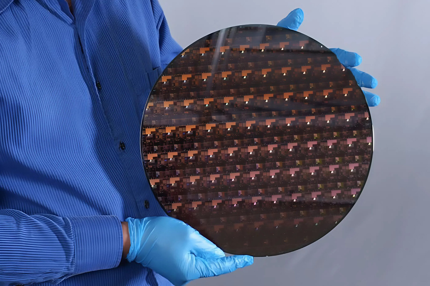
Strategically, restarting P5 is significant. The facility is designed for both foundry services and High-Bandwidth Memory (HBM) production, making it central to Samsung’s ambitions in the AI chip sector. HBM, being a critical component in AI accelerators, is a key competitive area in which Samsung has been striving to catch up with SK Hynix. The addition of a new HBM production line at P5 could meaningfully boost Samsung’s output and competitiveness in securing contracts with leading AI and tech firms.
The broader Pyeongtaek complex is set for six operational plants; P1 through P3 are already online, with P4 nearing completion, and P5 is now back under construction. Samsung’s renewed investment—highlighted by a $16.5 billion supply agreement with Tesla and potential new business with xAI—underscores a pivotal shift in its semiconductor strategy. By ramping up both AI chip and HBM production, Samsung is positioning itself at the forefront of the emerging AI hardware cycle and reinforcing its role as a central supplier in the ongoing AI revolution.
Source: South Korea